- 您现在的位置:买卖IC网 > Sheet目录3881 > PIC18F8585T-I/PT (Microchip Technology)IC PIC MCU FLASH 24KX16 80TQFP
PIC18F6585/8585/6680/8680
DS30491C-page 256
2004 Microchip Technology Inc.
19.6
A/D Conversions
Figure 19-3 shows the operation of the A/D converter
after the GO bit has been set and the ACQT2:ACQT0
bits are cleared. A conversion is started after the follow-
ing instruction to allow entry into Sleep mode before the
conversion begins.
Figure 19-4 shows the operation of the A/D converter
after the GO bit has been set, the ACQT2:ACQT0 bits
are set to ‘010’ and selecting a 4 TAD acquisition time
before the conversion starts.
Clearing the GO/DONE bit during a conversion will
abort the current conversion. The A/D Result register
pair will not be updated with the partially completed A/D
conversion sample. This means the ADRESH:ADRESL
registers will continue to contain the value of the last
completed conversion (or the last value written to the
ADRESH:ADRESL registers).
After the A/D conversion is completed or aborted, a
2TAD wait is required before the next acquisition can
be started. After this wait, acquisition on the selected
channel is automatically started.
19.7
Use of the CCP2 Trigger
An A/D conversion can be started by the “special event
trigger” of the CCP2 module. This requires that the
CCP2M3:CCP2M0 bits (CCP2CON<3:0>) be pro-
grammed as ‘1011’ and that the A/D module is enabled
(ADON bit is set). When the trigger occurs, the
GO/DONE bit will be set, starting the A/D conversion
and the Timer1 (or Timer3) counter will be reset to zero.
Timer1 (or Timer3) is reset to automatically repeat the
A/D acquisition period with minimal software overhead
(moving ADRESH/ADRESL to the desired location).
The appropriate analog input channel must be selected
and the minimum acquisition done before the “special
event trigger” sets the GO/DONE bit (starts a
conversion).
If the A/D module is not enabled (ADON is cleared), the
“special event trigger” will be ignored by the A/D
module but will still reset the Timer1 (or Timer3)
counter.
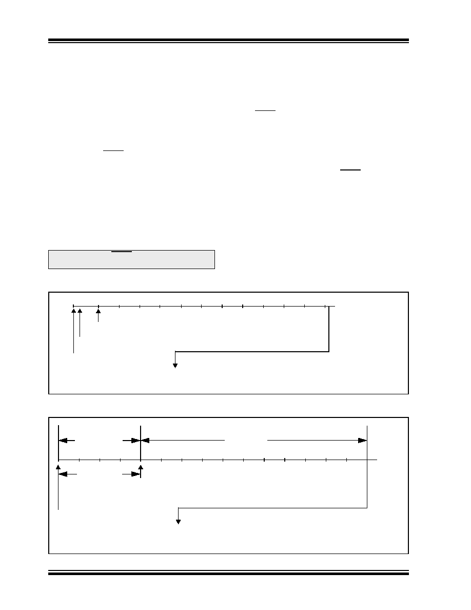
FIGURE 19-3:
A/D CONVERSION TAD CYCLES (ACQT<2:0> = 000, TACQ = 0)
FIGURE 19-4:
A/D CONVERSION TAD CYCLES (ACQT<2:0> = 010, TACQ = 4 TAD)
Note:
The GO/DONE bit should NOT be set in
the same instruction that turns on the A/D.
TAD1 TAD2 TAD3 TAD4 TAD5 TAD6 TAD7 TAD8
TAD11
Set GO bit
Holding capacitor is disconnected from analog input (typically 100 ns)
TAD9 TAD10
TCY - TAD
Next Q4: ADRESH/ADRESL is loaded, GO bit is cleared,
ADIF bit is set, holding capacitor is connected to analog input.
Conversion starts
b0
b9
b6
b5
b4
b3
b2
b1
b8
b7
1
2
3
4
5
6
7
8
11
Set GO bit
(Holding capacitor is disconnected)
9
10
Next Q4: ADRESH:ADRESL is loaded, GO bit is cleared,
ADIF bit is set, holding capacitor is reconnected to analog input.
Conversion starts
1
2
3
4
(Holding capacitor continues
acquiring input)
TACQT Cycles
TAD Cycles
Automatic
Acquisition
Time
b0
b9
b6
b5
b4
b3
b2
b1
b8
b7
发布紧急采购,3分钟左右您将得到回复。
相关PDF资料
XF2J-2424-11
CONN FPC 24POS 0.5MM SMT
PIC18LF6585T-I/PT
IC PIC MCU FLASH 24KX16 64TQFP
PIC18LF6680T-I/PT
IC PIC MCU FLASH 32KX16 64TQFP
XF2J-2224-11
CONN FPC 22POS 0.5MM SMT
PIC18F6525T-I/PT
IC PIC MCU FLASH 24KX16 64TQFP
PIC18F4439-E/ML
IC PIC MCU FLASH 6KX16 44QFN
XF2J-2024-11
CONN FPC 20POS 0.5MM SMT
PIC16LF747-I/ML
IC PIC MCU FLASH 4KX14 44QFN
相关代理商/技术参数
PIC18F85J10-I/PT
功能描述:8位微控制器 -MCU 32 KB FL 2 KB RAM RoHS:否 制造商:Silicon Labs 核心:8051 处理器系列:C8051F39x 数据总线宽度:8 bit 最大时钟频率:50 MHz 程序存储器大小:16 KB 数据 RAM 大小:1 KB 片上 ADC:Yes 工作电源电压:1.8 V to 3.6 V 工作温度范围:- 40 C to + 105 C 封装 / 箱体:QFN-20 安装风格:SMD/SMT
PIC18F85J10-I/PT
制造商:Microchip Technology Inc 功能描述:IC 8BIT MCU PIC18F 40MHZ TQFP-80 制造商:Microchip Technology Inc 功能描述:IC, 8BIT MCU, PIC18F, 40MHZ, TQFP-80
PIC18F85J10T-I/PT
功能描述:8位微控制器 -MCU 32 KB FL 2 KB RAM RoHS:否 制造商:Silicon Labs 核心:8051 处理器系列:C8051F39x 数据总线宽度:8 bit 最大时钟频率:50 MHz 程序存储器大小:16 KB 数据 RAM 大小:1 KB 片上 ADC:Yes 工作电源电压:1.8 V to 3.6 V 工作温度范围:- 40 C to + 105 C 封装 / 箱体:QFN-20 安装风格:SMD/SMT
PIC18F85J11-I/PT
功能描述:8位微控制器 -MCU 32KB Flash 2048BRAM 67I/O RoHS:否 制造商:Silicon Labs 核心:8051 处理器系列:C8051F39x 数据总线宽度:8 bit 最大时钟频率:50 MHz 程序存储器大小:16 KB 数据 RAM 大小:1 KB 片上 ADC:Yes 工作电源电压:1.8 V to 3.6 V 工作温度范围:- 40 C to + 105 C 封装 / 箱体:QFN-20 安装风格:SMD/SMT
PIC18F85J11T-I/PT
功能描述:8位微控制器 -MCU 32KB Flash 2048bytes-RAM 67I/O RoHS:否 制造商:Silicon Labs 核心:8051 处理器系列:C8051F39x 数据总线宽度:8 bit 最大时钟频率:50 MHz 程序存储器大小:16 KB 数据 RAM 大小:1 KB 片上 ADC:Yes 工作电源电压:1.8 V to 3.6 V 工作温度范围:- 40 C to + 105 C 封装 / 箱体:QFN-20 安装风格:SMD/SMT
PIC18F85J15-I/PT
功能描述:8位微控制器 -MCU 48 KB FL 4 KB RAM RoHS:否 制造商:Silicon Labs 核心:8051 处理器系列:C8051F39x 数据总线宽度:8 bit 最大时钟频率:50 MHz 程序存储器大小:16 KB 数据 RAM 大小:1 KB 片上 ADC:Yes 工作电源电压:1.8 V to 3.6 V 工作温度范围:- 40 C to + 105 C 封装 / 箱体:QFN-20 安装风格:SMD/SMT
PIC18F85J15T-I/PT
功能描述:8位微控制器 -MCU 48 KB FL 4 KB RAM RoHS:否 制造商:Silicon Labs 核心:8051 处理器系列:C8051F39x 数据总线宽度:8 bit 最大时钟频率:50 MHz 程序存储器大小:16 KB 数据 RAM 大小:1 KB 片上 ADC:Yes 工作电源电压:1.8 V to 3.6 V 工作温度范围:- 40 C to + 105 C 封装 / 箱体:QFN-20 安装风格:SMD/SMT
PIC18F85J50-I/PT
功能描述:8位微控制器 -MCU 32KB Flash 3936byte RAM RoHS:否 制造商:Silicon Labs 核心:8051 处理器系列:C8051F39x 数据总线宽度:8 bit 最大时钟频率:50 MHz 程序存储器大小:16 KB 数据 RAM 大小:1 KB 片上 ADC:Yes 工作电源电压:1.8 V to 3.6 V 工作温度范围:- 40 C to + 105 C 封装 / 箱体:QFN-20 安装风格:SMD/SMT